NCP1603
http://onsemi.com
27
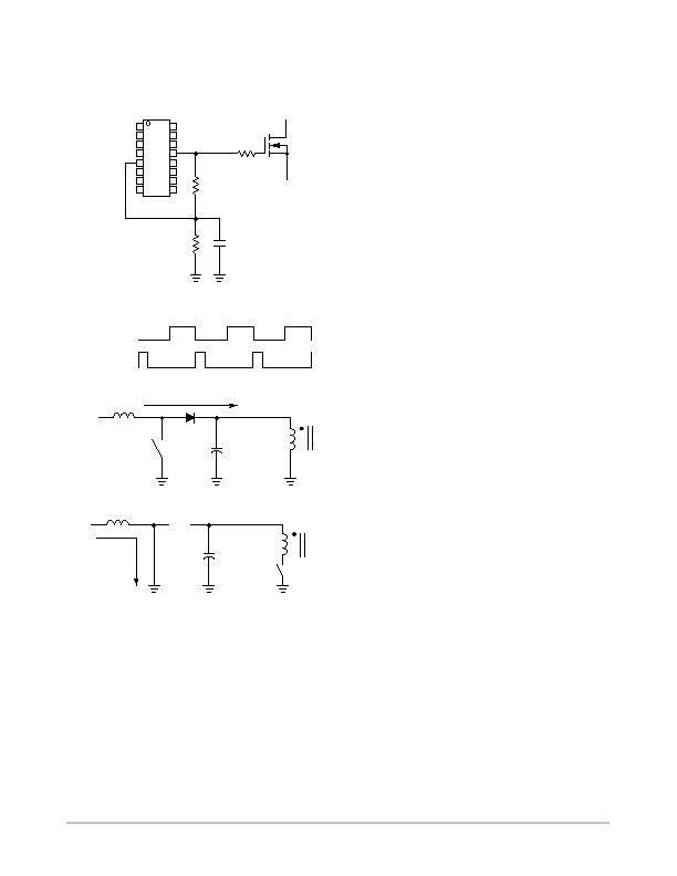
entering Osc pin and a capacitor is added to remove some
possible noise As a result, the current in Figure 73 may not
necessarily passes through the bulk capacitor for fewer
ripple current there.
Figure 72. Synchronization Configuration
OSC
Out2
Figure 73. Synchronization Timing Diagram
PWM drive
PFC drive
(DCM)
current
Phase 1
current
Phase 2
Output Drive
The output stages of the PFC section and PWM section are
designed for direct drive of power MOSFET. However, it is
recommended to connect a current limiting resistor to the gate
of the power MOSFET. The PFC section output is capable of
up to 500 mA and +750 mA peak drive current and has a
typical rise and fall time of 53 and 32 ns with a 1.0 nF load
while the PWM section output is capable of up to "1.0 A
peak drive current and has a typical rise and fall time of 40 ns
and a fall time of 15 ns with a 1.0 nF capacitive load.
Safety Features of NCP1603
(1) Bulk Voltage Overvoltage Protection (OVP)
When the PFC feedback current I
FB1
is higher than 107%
of the reference current I
ref
(i.e., the bulk voltage V
bulk
is
higher than 107% of its nominal value), the PFC Drive
Output pin (Pin 7) of the device goes low for protection and
the switch of the V
control
processing circuit is kept off. The
circuit automatically resumes operation when the output
voltage is lower than 107%.
The maximum OVP threshold is limited to 225 mA that
corresponds to 225 mA ?1.95 MW + 5.0 V = 443.75 V
when R
FB1
= 1.95 MW (e.g., 910 kW + 910 kW + 130 kW)
and V
FB1
= 5.0 V (for the worst case referring to
Figure 31). Hence, it is generally recommended to use
450 V rating output capacitor to allow some design margin.
(2) Bulk Voltage Undervoltage Protection (UVP)
When the PFC feedback current I
FB1
is smaller than 8%
of the reference current I
ref
, the PFC section is shutdown
and consumes less than 50 mA. In normal situation of the
boost converter configuration, the output bulk voltage
V
bulk
is always higher than input voltage V
in
and the I
FB1
is higher than 8% of the reference current. It enables the
PFC section to operate. Hence, UVP happens when the
bulk voltage V
bulk
is abnormally undervoltage, the FB1
pin (Pin 9) is opened, or the FB1 pin (Pin 9) is manually
pulled low.
(3) PFCStage Overcurrent Protection
When the PFC sense current I
S1
is higher than typically
200 mA, the PFC Drive Output (Pin 7) goes low. It
represents the PFCstage inductor current i
L
exceeds a
userdefined value. The operation automatically resumes
when the inductor current becomes lower than this
userdefined value at the next clock cycle.
(4) PWMStage ShortCircuit Protection
When V
FB2
remains higher than 3.0 V for 125 ms, a fault
is recognized. The PFCstage (i.e., V
aux
) will be disabled
and the V
CC2
will operate a double hiccup shown in
Figure 53. The operation will be selfrecovered if V
CC2
is
above 7.7 V and V
FB2
is below 3.0 V. This fault protection
is implemented by a timer and independent of badly
coupled auxiliary transformer winding.
(5) Latched V
CC
Overvoltage Protection
The normal operating voltage range of the CS2 pin
(Pin 3) is between 0 V and I
limit
(1.0 V typical). When the
voltage is above 1.0 V, the Out2 (Pin 13) goes low. When
the voltage increases above 3.0 V, the Out2 goes low and
stays latched off until the circuit is reset by unplugging
from main supply to make V
CC2
drop below V
CC(reset)
(4.0 V typical). This feature also offers the designer the
flexibility to implement an externally pullhigh latched
protection or latched shutdown circuit.
发布紧急采购,3分钟左右您将得到回复。
相关PDF资料
NCP1605DR2G
IC PFC CONTROLLER CCM/DCM 16SOIC
NCP1606BDR2G
IC POWER FACTOR CONTROLLER 8SOIC
NCP1607BDR2G
IC PFC CONTROLLER CRM 8SOIC
NCP1611BDR2G
IC PFC CTLR HE ENHANCED 8-SOIC
NCP1651DR2G
IC PFC CONTROLLER CCM/DCM 16SOIC
NCP1654BD133R2G
IC PFC CCM 133KHZ 8-SOIC
NCP1927DR2G
IC CTLR PFC/FLYBACK 16-SOIC
NCP380HMU21AATBG
IC CURRENT LIMIT SWITCH 6-UDFN
相关代理商/技术参数
NCP1605ADR2G
功能描述:功率因数校正 IC ENHANCED PFC CNTRLER RoHS:否 制造商:Fairchild Semiconductor 开关频率:300 KHz 最大功率耗散: 最大工作温度:+ 125 C 安装风格:SMD/SMT 封装 / 箱体:SOIC-8 封装:Reel
NCP1605BDR2G
功能描述:功率因数校正 IC High Volt Stby Mode Power Fact Corr Cont RoHS:否 制造商:Fairchild Semiconductor 开关频率:300 KHz 最大功率耗散: 最大工作温度:+ 125 C 安装风格:SMD/SMT 封装 / 箱体:SOIC-8 封装:Reel
NCP1605DR2G
功能描述:功率因数校正 IC Enhanced PFC HV and Eff Standby RoHS:否 制造商:Fairchild Semiconductor 开关频率:300 KHz 最大功率耗散: 最大工作温度:+ 125 C 安装风格:SMD/SMT 封装 / 箱体:SOIC-8 封装:Reel
NCP1605FORWGEVB
功能描述:电源管理IC开发工具 NCP1605 152 W FORWARD EVB
RoHS:否 制造商:Maxim Integrated 产品:Evaluation Kits 类型:Battery Management 工具用于评估:MAX17710GB 输入电压: 输出电压:1.8 V
NCP1605LCDTVGEVB
功能描述:BOARD EVAL NCP1605/1396 RoHS:是 类别:编程器,开发系统 >> 评估演示板和套件 系列:* 产品培训模块:Obsolescence Mitigation Program 标准包装:1 系列:- 主要目的:电源管理,电池充电器 嵌入式:否 已用 IC / 零件:MAX8903A 主要属性:1 芯锂离子电池 次要属性:状态 LED 已供物品:板
NCP1606ADR2G
功能描述:功率因数校正 IC PWR FCTR CONTROLLER RoHS:否 制造商:Fairchild Semiconductor 开关频率:300 KHz 最大功率耗散: 最大工作温度:+ 125 C 安装风格:SMD/SMT 封装 / 箱体:SOIC-8 封装:Reel
NCP1606APG
功能描述:功率因数校正 IC LO CST PWR FCTR CONT RoHS:否 制造商:Fairchild Semiconductor 开关频率:300 KHz 最大功率耗散: 最大工作温度:+ 125 C 安装风格:SMD/SMT 封装 / 箱体:SOIC-8 封装:Reel
NCP1606BDR2G
功能描述:功率因数校正 IC PWR FCTR CONTROLLER RoHS:否 制造商:Fairchild Semiconductor 开关频率:300 KHz 最大功率耗散: 最大工作温度:+ 125 C 安装风格:SMD/SMT 封装 / 箱体:SOIC-8 封装:Reel